Verilog interview Questions page 1    Verilog interview Questions Page 2
Verilog interview Questions page 3    Verilog interview Questions page 4
Verilog
gate level expected questions.
1) Tell something
about why we do gate level simulations?
a. Since scan and other test structures are added during and after
synthesis, they are not checked by the rtl simulations and therefore need to be
verified by gate level simulation.
b. Static timing analysis tools do not check asynchronous interfaces, so gate
level simulation is required to look at the timing of these interfaces.
c. Careless wildcards in the static timing constraints set false path or
mutlicycle path constraints where they don't belong.
d. Design changes, typos, or misunderstanding of the design can lead to
incorrect false paths or multicycle paths in the static timing constraints.
e. Using create_clock instead of create_generated_clock leads to incorrect
static timing between clock domains.
f. Gate level simulation can be used to collect switching factor data for power
estimation.
g. X's in RTL simulation can be optimistic or pessimistic. The best way to
verify that the design does not have any unintended dependence on initial
conditions is to run gate level simulation.
f. It's a nice "warm fuzzy" that the design has been implemented
correctly.
2)
Say if I perform Formal Verification say Logical Equivalence across Gatelevel
netlists(Synthesis and post routed netlist). Do you still see a reason behind
GLS.?
If we have verified the Synthesized netlist functionality is correct when compared to RTL and when we compare the Synthesized netlist versus Post route netlist logical Equivalence then I think we may not require GLS after P & R. But how do we ensure on Timing . To my knowledge Formal Verification Logical Equivalence Check does not perform Timing checks and dont ensure that the design will work on the operating frequency , so still I would go for GLS after post route database.
3)An
AND gate and OR gate are given inputs X & 1 , what is expected
output?
AND Gate output will be X
OR Gate output will be 1.
4)
What is difference between NMOS & RNMOS?
RNMOS is resistive nmos that is in simulation strength will decrease by one unit , please refer to below Diagram.

4)
Tell something about modeling delays in verilog?
Verilog can model delay types within its specification for gates and buffers. Parameters that can be modelled are T_rise, T_fall and T_turnoff. To add further detail, each of the three values can have minimum, typical and maximum values
T_rise, t_fall
and t_off
Delay modelling syntax follows a specific discipline;
gate_type #(t_rise, t_fall, t_off) gate_name (paramters);
When specifiying the delays it is not necessary to have all of the delay values
specified. However, certain rules are followed.
and #(3) gate1 (out1, in1,
in2);
When only 1 delay is specified, the value is used to represent all of the delay
types, i.e. in this example, t_rise = t_fall = t_off = 3.
or #(2,3) gate2 (out2, in3,
in4);
When two delays are specified, the first value represents the rise time, the
second value represents the fall time. Turn off time is presumed to be 0.
buf #(1,2,3) gate3 (out3,
enable, in5);
When three delays are specified, the first value represents t_rise, the second
value represents t_fall and the last value the turn off time.
Min, typ and max values
The general syntax for min, typ and max delay modelling is;
gate_type #(t_rise_min:t_ris_typ:t_rise_max, t_fall_min:t_fall_typ:t_fall_max, t_off_min:t_off_typ:t_off_max)
gate_name (paramteters);
Similar rules apply for th especifying order as above. If only one t_rise value is specified then this value is applied to min, typ and max. If specifying more than one number, then all 3 MUST be scpecified. It is incorrect to specify two values as the compiler does not know which of the parameters the value represents.
An example of specifying two
delays;
and #(1:2:3, 4:5:6) gate1 (out1, in1, in2);
This shows all values necessary for rise and fall times and gives values for
min, typ and max for both delay types.
Another acceptable
alternative would be;
or #(6:3:9, 5) gate2 (out2, in3, in4);
Here, 5 represents min, typ and max for the fall time.
N.B. T_off is only applicable to tri-state logic devices, it does not apply to primitive logic gates because they cannot be turned off.
5)
With a specify
block how to defining pin-to-pin delays for the module ?
module A( q, a, b, c, d )
input a, b, c, d;
output q;
wire e, f;
// specify block containing delay statements
specify
( a => q ) = 6; // delay from a to q
( b => q ) = 7; // delay from b to q
( c => q ) = 7; // delay form c to q
( d => q ) = 6; // delay from d to q
endspecify
// module definition
or o1( e, a, b );
or o2( f, c, d );
exor ex1( q, e, f );
endmodule
module A( q, a, b, c, d )input a, b, c, d;output q;wire e, f;// specify block containing full connection statementsspecify( a, d *> q ) = 6; // delay from a and d to q( b, c *> q ) = 7; // delay from b and c to qendspecify// module definitionor o1( e, a, b );or o2( f, c, d );exor ex1( q, e, f );endmodule
6)
What are conditional path delays?
Conditional path delays, sometimes called state dependent path delays, are used to model delays which are dependent on the values of the signals in the circuit. This type of delay is expressed with an if conditional statement. The operands can be scalar or vector module input or inout ports, locally defined registers or nets, compile time constants (constant numbers or specify block parameters), or any bit-select or part-select of these. The conditional statement can contain any bitwise, logical, concatenation, conditional, or reduction operator. The else construct cannot be used.
//Conditional path delaysModule A( q, a, b, c, d );output q;input a, b, c, d;wire e, f;// specify block with conditional timing statementsspecify// different timing set by level of input aif (a) ( a => q ) = 12;if ~(a) ( a => q ) = 14;// delay conditional on b and c// if b & c is true then delay is 7 else delay is 9if ( b & c ) ( b => q ) = 7;if ( ~( b & c )) ( b => q ) = 9;// using the concatenation operator and full connectionsif ( {c, d} = 2'b10 ) ( c, d *> q ) = 15;if ( {c, d} != 2'b10 ) ( c, d *> q ) = 12;endspecifyor o1( e, a, b );or o2( f, c, d );exor ex1( q, e, f );endmodule
6) Tell something about Rise, fall, and turn-off delays?
Timing delays between pins can be expressed in greater detail by specifying rise, fall, and turn-off delay values. One, two, three, six, or twelve delay values can be specified for any path. The order in which the delay values are specified must be strictly followed.
// One delay used for all transitionsspecparam delay = 15;( a => q ) = delay;// Two delays gives rise and fall timesspecparam rise = 10, fall = 11;( a => q ) = ( rise, fall );// Three delays gives rise, fall and turn-off// rise is used for 0-1, and z-1, fall for 1-0, and z-0, and turn-off for 0-z, and 1-z.specparam rise = 10, fall = 11, toff = 8;( a => q ) = ( rise, fall, toff );// Six delays specifies transitions 0-1, 1-0, 0-z, z-1, 1-z, z-0// strictly in that orderspecparam t01 = 8, t10 = 9, t0z = 10, tz1 = 11, t1z = 12, tz0 = 13;( a => q ) = ( t01, t10, t0z, tz1, t1z, tz0 );// Twelve delays specifies transitions:// 0-1, 1-0, 0-z, z-1, 1-z, z-0, 0-x, x-1, 1-x, x-0, x-z, z-x// again strictly in that orderspecparam t01 = 8, t10 = 9, t0z = 10, tz1 = 11, t1z = 12, tz0 = 13;specparam t0x = 11, tx1 = 14, t1x = 12, tx0 = 10, txz = 8, tzx = 9;( a => q ) = ( t01, t10, t0z, tz1, t1z, tz0, t0x, tx1, t1x, tx0, txz, tzx );
7)Tell me about In verilog delay modeling?
Distributed Delay
Distributed delay is delay assigned to each gate in a module. An example circuit is shown below.
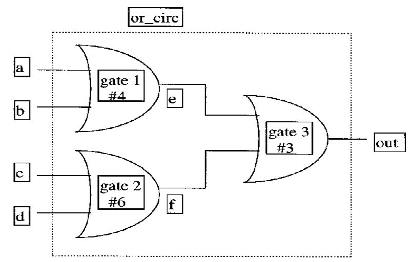
Figure 1: Distributed delay
As can be seen from Figure 1, each of the or-gates in the circuit above has a delay assigned to it:
gate 1 has a delay of 4
gate 2 has a delay of 6
gate 3 has a delay of 3
When the input of any gate change, the output of the gate changes after the delay value specified.
The gate function and delay, for example for gate 1, can be described in the following manner:
or #4 a1 (e, a, b);
A delay of 4 is assigned to the or-gate. This means that the output of the gate, e, is delayed by 4 from the inputs a and b.
The module explaining Figure 1 can be of two forms:
1)Version 1 models the circuit by assigning delay values to individual gates, while version 2 use delay values in individual assign statements. (An assign statement allows us to describe a combinational logic function without regard to its actual structural implementation. This means that the assign statement does not contain any modules with port connections.)
The above or_circ modules results in delays of (4+3) = 7 and (6+3) = 9 for the 4 connections part from the input to the output of the circuit.
Lumped Delay
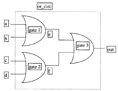
Lumped delay is delay assigned as a single delay in each module, mostly to the output gate of the module. The cumulative delay of all paths is lumped at one location. The figure below is an example of lumped delay. This figure is similar as the figure of the distributed delay, but with the sum delay of the longest path assigned to the output gate: (delay of gate 2 + delay of gate 3) = 9.

Figure 2: Lumped delay
As can be seen from Figure 2, gate 3 has got a delay of 9. When the input of this gate changes, the output of the gate changes after the delay value specified.
The program corresponding to Figure 2, is very similar to the one for distributed delay. The difference is that only or - gate 3 has got a delay assigned to it:
1)This model can be used if delay between different inputs is not required.
Pin - to Pin Delay
Pin - to - Pin delay, also called path delay, is delay assigned to paths from each input to each output. An example circuit is shown below.
The total delay from each input to each output is given. The same example circuit as for the distributed and lumped delay model is used. This means that the sum delay from each input to each output is the same.
The module for the above circuit is shown beneath:
Module or_circ (out, a, b, c, d);Path delays of a module are specified incide a specify block, as seen from the example above. An example of delay from the input, a, to the output, out, is written as (a => out) = delay, where delay sets the delay between the two ports. The gate calculations are done after the path delays are defined.
For larger circuits, the pin
- to - pin delay can be easier to model than distributed delay. This is because
the designer writing delay models, needs to know only the input / output pins
of the module, rather than the internals of the module. The path delays for
digital circuits can be found through different simulation programs, for
instance SPICE. Pin - to - Pin delays for standard parts can be found from data
books. By using the path delay model, the program speed will increase.
Delay Modeling: Timing Checks.
Keywords: $setup, $hold, $width
This section, the final part of the delay modeling chapter, discusses some of the various system tasks that exist for the purposes of timing checks. Verilog contains many timing-check system tasks, but only the three most common tasks are discussed here: $setup, $hold and $width. Timing checks are used to verify that timing constraints are upheld, and are especially important in the simulation of high-speed sequential circuits such as microprocessors. All timing checks must be contained within specify blocks as shown in the example below.
The $setup and $hold tasks are used to monitor the setup and hold constraints during the simulation of a sequential circuit element. In the example, the setup time is the minimum allowed time between a change in the input d and a positive clock edge. Similarly, the hold time is the minimum allowed time between a positive clock edge and a change in the input d.
The $width task is used to check the minimum width of a positive or negative-going pulse. In the example, this is the time between a negative transition and the transition back to 1.

Syntax:
NB: data_change, reference and reference1 must be declared wires.
$setup(data_change, reference, time_limit);
data_change: signal that is checked against the reference
reference: signal used as reference
time_limit: minimum time required between the two events.
Violation if: Treference - Tdata_change < time_limit.
$hold(reference, data_change, time_limit);
reference: signal used as reference
data_change: signal that is checked against the reference
time_limit: minimum time required between the two events.
Violation if: Tdata_change - Treference < time_limit
$width(reference1, time_limit);
reference1: first transition of signal
time_limit: minimum time required between transition1 and transition2.
Violation if: Treference2 - Treference1 < time_limit
Example:
module d_type(q, clk, d); output q; input clk, d; reg q; always @(posedge clk) q = d; endmodule // d_type module stimulus; reg clk, d; wire q, clk2, d2; d_type dt_test(q, clk, d); assign d2=d; assign clk2=clk; initial begin $display ("\t\t clock d q"); $display ($time," %b %b %b", clk, d, q); clk=0; d=1; #7 d=0; #7 d=1; // causes setup violation #3 d=0; #5 d=1; // causes hold violation #2 d=0; #1 d=1; // causes width violation end // initial begin initial #26 $finish; always #3 clk = ~clk; always #1 $display ($time," %b %b %b", clk, d, q); specify $setup(d2, posedge clk2, 2); $hold(posedge clk2, d2, 2); $width(negedge d2, 2); endspecifyendmodule // stimulus
Output:
clock d q 0 x x x 1 0 1 x 2 0 1 x 3 1 1 x 4 1 1 1 5 1 1 1 6 0 1 1 7 0 0 1 8 0 0 1 9 1 0 1 10 1 0 0 11 1 0 0 12 0 0 0 13 0 0 0 14 0 1 0 15 1 1 0 "timechecks.v", 46: Timing violation in stimulus $setup( d2:14, posedge clk2:15, 2 ); 16 1 1 1 17 1 0 1 18 0 0 1 19 0 0 1 20 0 0 1 21 1 0 1 22 1 1 0 "timechecks.v", 47: Timing violation in stimulus $hold( posedge clk2:21, d2:22, 2 ); 23 1 1 0 24 0 0 0 25 0 1 0 "timechecks.v", 48: Timing violation in stimulus $width( negedge d2:24, : 25, 2 );
9) Draw a 2:1 mux using switches and verilog code for it?
1-bit 2-1 Multiplexer
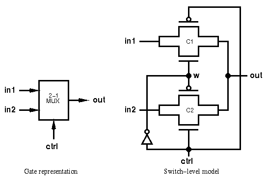
This circuit assigns the output out to either inputs in1 or in2 depending on the low or high values of ctrl respectively.
// Switch-level description of a 1-bit 2-1 multiplexer// ctrl=0, out=in1; ctrl=1, out=in2 module mux21_sw (out, ctrl, in1, in2); output out; // mux output input ctrl, in1, in2; // mux inputs wire w; // internal wire inv_sw I1 (w, ctrl); // instantiate inverter module cmos C1 (out, in1, w, ctrl); // instantiate cmos switches cmos C2 (out, in2, ctrl, w); endmodule
An inverter is required in the multiplexer circuit, which is instantiated from the previously defined module.
Two transmission gates, of
instance names C1 and C2, are implemented with the cmos statement, in
the format cmos
[instancename]([output],[input],[nmosgate],[pmosgate]). Again, the instance name is
optional.
10)What
are the synthesizable gate level constructs?

The above table gives all the gate level constructs of only the constructs in first two columns are synthesizable.